

Underlying the hype for SiC (silicon carbide) and the future potential of GaN (gallium nitride) for EV power electronics, challenges remain for both technologies. While OEMs, tier-one suppliers, and market analysts generally agree that SiC and GaN will eventually share the market with incumbent Si technologies, the exact roadmap and time scale remain uncertain. A development in its relative infancy that IDTechEx expects to boost overall performance, volume capabilities, and cost, are engineered substrates. IDTechEx’s report, “Power Electronics for Electric Vehicles 2025-2035: Technologies, Markets, and Forecasts”, assesses the potential upsides and challenges to using engineered substrates for EV power electronics, including scalability, production volumes, and performance.
Substrates are traditionally thin discs of monocrystalline semiconductor material on which devices, such as MOSFETs and IGBTs, are grown. Since the epitaxial growth of the semiconductor is built on this base, ideally, the substrate is the same crystal as that of epitaxy (homoepitaxy), e.g., Si substrate for Si devices, etc. For Si MOSFETs and IGBTs, used in power electronics in automotive modules, such as the onboard charger, traction inverter, and DC-DC converter, the obvious choice is Si substrates. Global suppliers include SUMCO, Shin-Etsu, and GlobalWafers, with the bottom line being that the technology is mature, reliable, and cost-effective.
Boosting SiC MOSFET volumes with engineered substrates
The SiC wafer market has only recently started to globalize, with approximately 75% of SiC wafers being produced in the US as of 2023. With companies such as Wolfspeed and STMicroelectronics expanding into Europe and China, the emergence of other SiC wafer companies, and the transition from 150mm to 200mm substrates, the market is slated to become more competitive, driving costs down.
In parallel to these developments, companies are creating engineered substrates for SiC power devices. Generally, these leverage silicon-on-insulator (SOI) technologies and consist of a polycrystalline SiC layer bonded to a thin layer of monocrystalline SiC (a SiC wafer is typically wholly monocrystalline SiC). Companies leveraging some variant of this technology include Soitec, which has previously announced collaborations with X-FAB and STMicroelectronics, and Sicoxs (a subsidiary of Sumitomo Metal Mining), which currently markets 6-inch engineered SiC substrates and expects mass production in the fiscal year 2025.
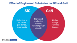
With the globalization of the SiC substrate market and an increasing number of players, automotive OEMs are seeking large volumes of SiC MOSFETs to create efficient powertrains, which can increase the range of a vehicle by 7% compared to Si IGBTs. In terms of volume and cost, engineered substrates have advantages and can result in production volumes an order of magnitude greater than without engineered substrates using the same amount of monocrystalline SiC. To create engineered substrates, a mechanically strong polycrystalline SiC wafer is prepared, with steps including grinding and polishing to get it flat, from which a very thin layer of monocrystalline SiC substrate is strongly bonded to the polycrystalline wafer. After processing, activation, and inspection, the engineered substrate is ready, and the rest of the monocrystalline wafer will be reused to manufacture more engineered substrates.
This results in reduced costs, with SiC substrates taking up to 50% of a total device’s cost and increased volume, with one monocrystalline SiC wafer now able to produce 10-50 substrates. It has also been shown that engineered substrates have a lower ‘on resistance’ over the substrate area, resulting in less heat generated per unit area and the potential for a greater number of chips produced per substrate.
While engineered SiC substrates show potential, it will still take a couple of years for them to be in mass production, and questions remain over the main form of commercialization for them. For example, companies could license out the bonding process, partner with foundries or device companies to produce substrates at scale or loan out the necessary equipment. Design cycles and lead times in the automotive industry are notoriously long, spanning multiple years. In addition, high requirements and extensive testing are needed to qualify these processes to make devices for EVs.
Engineered substrates to make GaN viable in traction inverters
Since SiC is already used in EV power electronics, the mass commercialization of engineered substrates would help accelerate that development. In the case of GaN, multiple companies, such as Vitesco and VisIC Technologies, are looking to release high-voltage automotive GaN products, but the obstacles are slightly different. IDTechEx is aware of only one company, Odyssey Semiconductor, that produces bulk GaN substrates for GaN devices. In May 2024, it was acquired by Power Integrations, but it remains to be seen whether GaN substrates can be manufactured reliably and cost-effectively.
Historically, silicon substrates have been used to grow GaN devices (heteroepitaxy), and almost every device on the market uses silicon substrates. Since silicon substrates are already in mass production for silicon-based devices, their use for GaN transistors seems like a no-brainer. Buffer layers manage the strain and lattice mismatch between the epitaxial GaN and Si substrate, improving robustness. However, GaN can still only be grown in thin layers on Si substrates, resulting in greater defectivity than homoepitaxial GaN and voltage-limited lateral GaN devices
For GaN to be used in the traction inverter, devices need to be capable of sustaining high voltages and power for extended periods, which is where current GaN technologies fall short. Alternatives include GaN-on-sapphire and GaN-on-SiC, which can yield higher voltage devices but are not compatible with CMOS processes, are expensive and have other issues with handling and thermal performance. Engineered GaN substrates mitigate these issues by creating a substrate that minimizes lattice mismatch and aligns the thermal expansion coefficient with that of GaN to produce thicker epitaxial layers of GaN for vertical devices going beyond 1200V. This is the approach taken by the fabless company Qromis, with its QST (Qromis Substrate Technology). By matching the substrate’s physical properties with GaN, devices will have low defectivity and minimize breakages. Furthermore, while current GaN devices are grown on 150mm Si substrates, engineered substrates are scalable, future-proofing GaN to be grown on 200mm and eventually 300mm substrates. This will, in time, increase production volumes and decrease the cost per device.
With GaN substrates currently being prohibitively expensive, the next best thing is to manufacture something as similar as possible to GaN, which is what engineered substrates aim to do. Si substrates are cost-effective with guaranteed large volumes but struggle to meet the demands of high-voltage power electronics using current technology. Alternative substrates such as SiC and sapphire come with other drawbacks, therefore engineered substrates could be a key technology in enabling GaN to enter the EV power electronics market. However, IDTechEx is not aware of any current adoption plans from automotive OEMs or tier-one suppliers
To summarize, engineered substrates will open the path to vertical GaN devices and can make devices reliable, more cost-effective, scalable, and power-dense. IDTechEx conducts further analysis on engineered substrates in their “Power Electronics for Electric Vehicles 2025-2035: Technologies, Markets, and Forecasts” report and compares its impact to other developments in EV power electronics, such as integrated power electronics and 3-level inverters


